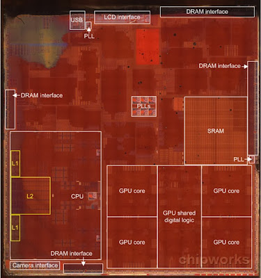
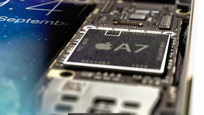
As evident from the image above, the new chip companies everything – RAM, controllers, cache, memory, shared logic etc. Chipworks also said that the dual-core CPU had the design from ARM v8 (Apple’s) architecture, and was not a design licensed from ARM A53/57. This core uses 256 KB L1 cache and 1 MB L2 cache. The graphic processor has four cores.
The dual-core CPU and cache make up ~17 percent of the die area, and the quad-core GPU and shared logic about 22 percent.
The source says for the Secure Enclave:
Actually, if we compare it with the A6, that may not be such a stupid idea – there is no comparable block that I can see in there.
I wouldn’t have thought that a fingerprint scan would create that much data, but given that multiple scans have to be stored, and in any orientation, maybe that much storage is needed.
One thing we do know is that it’s the biggest fingerprint sensor that we’ve seen so far, coming in at ~39 mm².
Here’s a screenshot showing Secure Enclave
Chipworks says that Secure Enclave as 3MB storage, is situated above the GPU cluster, and is essentially an SRAM.
A7 also has few similarities with previous A6X, A6 and A5 processors such as camera interface, USB and LCD. The company will also be telling more about Touch ID later.
At the moment, Samsung doesn’t have any plans to introduce this technology, as an official told The Korean Herald.


